36V High Efficiency Boost Converter with I2C Controlled 6-CH LED Driver
Abstract
The RT4539 device provides a highly integrated white LED driver solution for notebook and Tablet LCD backlight. The device is a white-LED driver featuring a 36V high efficiency asynchronous boost converter and six 35mA high precision current sinks with a maximum of ±2% current mismatching for excellent brightness uniformity in each string of LEDs. The RT4539 has five dimming modes including DC mode, direct PWM mode, PWM-26k mode, mix mode and mix-26K mode that can be controlled by PWM signal or an I2C master, or both. In addition, The RT4539 has a wide input voltage operating range from 2.7V to 24V and contains I2C interface for controlling the dimming mode, operating frequency, LED current slope time and the LED current. It is suitable for single/two cell battery input to drive LED light bars which contain six strings in parallel.
1.
Brightness Control
Function
1.1 Advanced Brightness
Control
There are three ways to control the current of Current sink channels: by external PWM signal or an I2C master, or both as shown in Table 1. The PWM generator internally detects the duty cycle at the PWM pin, register or both and then it uses internal oscillator to generate a PWM data of a specific frequency. In addition, the PWM data will calculate via the PWM curve-shaper path and dimming function path which determines dimming Mode and kinds of LED current slope curve. In direct PWM mode, all current feedback channels are turned on and off and are synchronized with the input PWM signal.
Table 1. Setting Advanced Brightness Control
|
Address
|
Bit
|
Name
|
Default Value
|
Description
|
R/W
|
|
07h
|
[1:0]
|
Advanced brightness control
|
External PWM signal (B00)
|
B00: External PWM signal
B01: I2C brightness register (04h, 05h)
B10: External PWM signal multiplied with I2C brightness register (04h, 05h)
|
R/W
|
2.
Power-On Sequence
2.1 Power-On Sequence by PWM Input Brightness Control Mode
When EN is above the minimal operational value, the RT4539 enters start-up mode. During start-up mode, an VCP Voltage starts to ramp up and then EEPROM values loads to registers once VCP reaches power satisfactory level (POR). I2C is available after the start-up sequence has ended.
In standby mode, the device waits for the BL_EN bit to go high to start the boost start-up sequence. Also, in standby mode the PWM input duty cycle signal is active. Moreover, the user can also set LED related configuration and functions via I2C interface.
Once the BL_EN bit is set to 1, boost starts working, and the device enters normal mode with brightness set by PWM input duty cycle signal. If no brightness is set, the backlight stays in the same state continuously until PWM signal receives at least two PWM pulses.
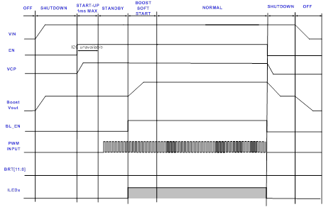
Figure 1. Start-Up and Shutdown with PWM Input Brightness Control
2.2 Power-On Sequence by I2C Brightness Control Mode
When EN is above the minimum operational value, the RT4539 enters start-up mode. During start-up mode, an VCP voltage starts to ramp up and then EEPROM values load to registers once VCP reaches power satisfactory level (POR). I2C is available after the start-up sequence has ended.
In standby mode, the device waits for the BL_EN bit to go high to start the boost start-up sequence. Also, in standby mode I2C is active, and brightness or other configuration registers can write via I2C interface.
Once the BL_EN is set to 1, boost starts working, and device enters normal mode with brightness set by I2C brightness registers. If no brightness is set, the backlight stays at the same state continuously until the brightness value writes to the I2C register.
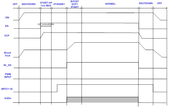
Figure 2. Start-Up and Shutdown with I2C Brightness Control
2.3 Power-On Sequence by I2C Control + PWM Input Brightness Control Mode
When EN is above the minimum operational value, the RT4539 enters start-up mode. During start-up mode an VCP voltage starts to ramp up and then EEPROM values loads to registers once VCP reaches power satisfactory level (POR). I2C is available after the start-up sequence has ended.
In standby mode, the RT4539 waits for the BL_EN to go high to start the boost start-up sequence. Also, in standby mode I2C registers can write and PWM input duty cycle signal is active; in this mode, the LED current will be PWM duty cycle plus I2C Code.
Once the BL_EN bit is set to 1, boost starts working, and device enters normal mode with brightness set by the PWM input duty cycle multiplied by I2C brightness register value. If no brightness is set, backlight stays at the same state continuously until I2C brightness register receives value and PWM signal receives atleast two PWM pulses.
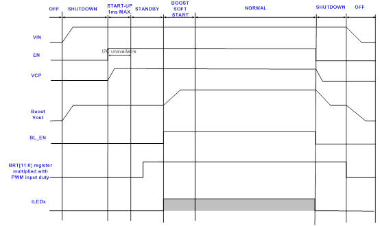
Figure 3. Start-Up and Shutdown with I2C + PWM Input Brightness Control
3. Dimming Mode
3.1 Dimming Mode Selection
The RT4539 provides five dimming modes for controlling the LED brightness. These functions include PWM mode, PWM-26k Mode, Mixed Mode, Mixed-26k Mode, and DC mode. The dimming control mode selection is programmable by register address 00h.
Table 2. Dimming Control Mode Selection
|
Address
|
Bit
|
Name
|
Default Value
|
Description
|
R/W
|
|
00h
|
[2:0]
|
Diming mode selection
|
Mixed-26kHz mode (B011)
|
B000: PWM mode (Direct PWM)
B001: PWM-26k mode (Non-Direct PWM)
B010: Mixed mode
B011: Mixed-26kHz mode
B1xx: DC mode
|
R/W
|
Current sink channels current must program to the highest WLED current expected; each current sink channel current is programmable together from 10.04mA to 35mA by an EEPROM register through the I2C interface. The maximum current is programmable by register address 02h.
The brightness can be controlled using an external PWM signal, the brightness registers are accessible by users via an I2C interface or both. For the register control method, the 8bits in address 0x05h register (LSB) along the 4bits defined in address 0x04h register (MSB) allow LED brightness to be set in 12-bit fine steps. For the external PWM signal, the Brightness depends on PWM duty cycles.
3.2 PWM
Mode
PWM control is the traditional way of controlling the brightness using PWM of the outputs with the same LED current across the entire brightness range. Brightness control is achieved by varying the duty cycle proportional to the input PWM as shown in Figure 4 below. In PWM mode, the PWM dimming frequency is synchronized with the input PWMI frequency. The LED maximum current of each channel and related LED functions can be set by I2C interface. The following Figure 4. is PWM mode behavior waveform. For example, LED maximum current is 20mA, if PWM duty cycle is 50%, the current sink output average current will be 10mA.
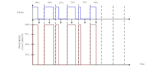
Figure 4. PWM Mode Behavior
The ON/OFF of the current source is synchronized to the PWM signal. The frequency of LED current is equal to the PWM input signal.
3.3 PWM-26k
Mode
When user chooses PWM-26k dimming mode, the PWM output frequency will be fix as below Table 3 which can division five different frequency via I2C interface. Brightness control is achieved by varying the duty cycle proportional to the input PWM as below figure 5. Moreover, the 26kHz mode division frequency function only be used at PWM input control, if input control interface is I2C mode, the address 08h [7:5] must write B000.
Table 3. 26kHz Mode Division Frequency
|
Address
|
Bit
|
Name
|
Default Value
|
Description
|
Resolution
|
R/W
|
|
08h
|
[7:5]
|
26kHz mode division frequency
|
26kHz
|
PWMO frequency
B000: 26kHz
B001: 26kHz/2
B010: 26kHz/4
B011: 26kHz/8
B1xx: 26kHz/16
|
--
|
R/W
|
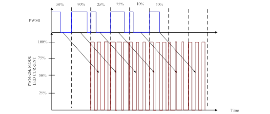
Figure 5. PWM-26k Mode Behavior
The LED current will have two-cycle delay in this mode, while the delay cycles are for average current calculation.
3.4 Mixed
Mode
Mixed mode dimming combines PWM and DC modes for current sink current control. By using mix dimming, dimming ratio will be increased 4 times. In mix mode, PWM dimming is used for low brightness range of brightness, and DC dimming is used for high brightness levels as shown in Figure 6. Mixed-mode dimming provides the benefits of both the DC and PWM dimming. For 25% < PWM Duty < 100%, DC dimming benefits the low power requirement and increases the power to brightness transform efficiency. At light load conditions, PWM Duty < 25%, the PWM dimming provides both high accuracy brightness and low color distortion. In addition, For PWM Duty < 25%, each current sink turns on duty will be increased 4 times at translated duty cycle and same frequency to the input PWM, and in the LED on duty current is regulated at 25% of full scale. Moreover, The PWM and current modes transition threshold can be set at 25% or at 12.5% brightness.
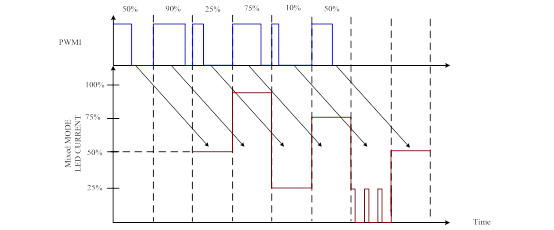
Figure 6. Mixed Mode Behavior
The LED current will have two-cycle delay in this mode, while the delay cycles are for average current calculation.
When 25% ≤ PWM duty ≤ 100%, the current source outputs are DC dimming, and the PWM duty cycle modulates the amplitude of the currents in 100% dimming.
PWM duty < 25%, the DC dimming will translate to PWM dimming, controlling the PWM duty instead by amplitude. The LED current is fixed on quarter of LED current setting.
3.5 Mixed-26k
Mode
When the user chooses Mixed-26k mode dimming, all behaviors are the same Mix mode, except PWM dimming output frequency. If PWM duty is lower than transition threshold point, the PWM dimming frequency is set to the 26kHz mode division frequency. Moreover, 26kHz mode division frequency function can only be used at PWM input control; if input control interface is I2C mode, the address 08h [7:5] must write B000.
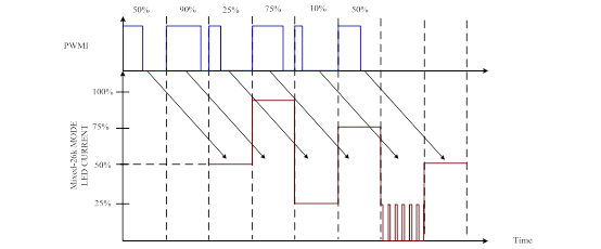
Figure 7. Mixed-26k Mode Behavior
The LED current will have two-cycle delay in this mode, while the delay cycles are for average current calculation.
When 25% ≤ PWM duty ≤ 100%, the current source outputs are DC dimming, and the PWM duty cycle modulates the amplitude of the currents in 100% dimming.
PWM duty < 25%, the DC dimming will translate to PWM dimming, controlling the PWM duty instead by amplitude. The LED current is fixed on quarter of LED current setting.
3.6 DC
Mode
In DC mode, RT4539 features pure analog dimming all over the brightness range of full-scale LED current. DC dimming can provide potentially low power requirement for same WLED brightness output because of low voltage drop across each LED when the current is low. In DC mode, brightness control is achieved by changing the LED current proportionally from maximum value to a minimum value across the entire brightness range. The LED current of each channel can be set by I2C interface, and the maximum LED current setting is 35mA. The one-step of LED current is approximately 0.12mA. Current resolution in this mode is 12bits.
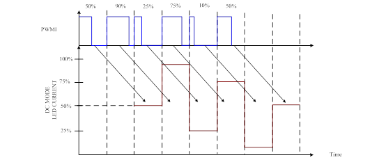
Figure 8. DC Mode Behavior
The LED current will have two-cycle delay in this mode, while the delay cycles are for average current calculation.
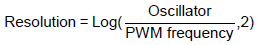
3.7 Resolution
3.7.1 Resolution
The RT4539 equips various dimming modes including PWM Mode, PWM-26k mode, Mixed Mode, Mixed-26k mode and DC Mode. If DC mode is selected, the maximum resolution will be 12bit and other resolution can eventually be determined according to equation 1. But in mix mode and mix mode-26k, the resolution will relate with PWM transition threshold point, for example, when PWM transient threshold point sets 25%, the resolution will be 11bit during PWM duty < 25%. When transient point sets 12.5%, the resolution will be 12bit during PWM duty < 12.5%. In addition, the following Table 4. describes resolution of each mode.
Table 4. Each Dimming Mode Resolution by 26kHz PWM Frequency
|
Oscillator = 16M
|
LED Frenquency = 26kHz
|
|
Brightmess < 25%
(Set threshold is 25%)
|
Brightmess > 25%
(Set threshold is 25%)
|
Brightmess < 12.5%
(Set threshold is 12.5%)
|
Brightmess > 12.5%
(Set threshold is 12.5%)
|
|
PWM Mode
|
According to input PWM frequency to calculate resolution.
|
|
PWM-26k Mode
|
9 bit
|
12 bit
|
9 bit
|
12 bit
|
|
Mixed Mode
|
According to input PWM frequency to calculate resolution.
Calculate resolution +2bit
|
12 bit
|
According to input PWM frequency to calculate resolution.
Calculate resolution +3bit
|
12 bit
|
|
Mixed-26k Mode
|
9+2 bit
|
12 bit
|
9+3 bit
|
12 bit
|
|
DC Mode
|
12 bit
|
12 bit
|
(1)
The following figures show the resolution of PWM at different transition point.
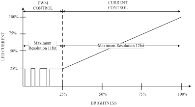
Figure 9. Duty Change Threshold is 25% in Mixed and Mixed-26k Mode
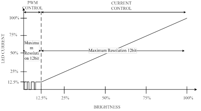
Figure 10. Duty Change Threshold is 12.5% in Mixed and Mixed-26k Mode
3.8 Linear
and Exponential Function
The RT4539 equips ILED Mapping mode including linear and exponential functions. In linear mapping mode, the dimming settings presented either via the PWM input or registers are translated linearly into the LED current. For a better visual experience, The RT4539 can also translate the dimming settings via an exponential mapping to produce the LED current. Moreover, the exponential function is valid for DC mode only and an example is shown in the following Figure 11.
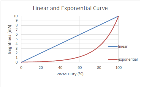
Figure 11. Linear and Exponential Curve
3.8.1 Exponential Function Example
3.8.1.1 External PWM Signal
LED brightness mapping can be selected to be either linear or exponential (DC mode only) by address 0x03h [7].
When address 0x07h is set to B00 and exponential mode is selected by address 0x03h, the PWM duty will transfer cycle-to-current response with 11-bit resolution and target ILED is approximated by the following equation:
ILED = 50μA × 1.00304 2047 × PWM duty (for PWM duty ≠ 0) @ ILEDmax = 25mA
It is valid for PWM duty cycles within 0 to 100%. If duty cycle is 0, the brightness will be disabled.
3.8.1.2 External PWM Signal
When address 0x07h is set to B01 and exponential mode is selected by address 0x03h, the I2C interface will transfer code-to-current response with 11-bit resolution and target ILED is approximated by the following equation:
ILED = 50μA × 1.00304I2C code (for codes>0) @ ILEDmax = 25mA
This equation is valid for I2C brightness codes between 1 and 2047. If Code is 0, the brightness will be disabled.
3.8.2 Linear Example
3.8.2.1 External PWM Signal
When address 0x07h is set to B00 and linear mode is selected by address 0x03h, the PWM duty will transfer cycle-to-current response with 12-bit resolution and target ILED is approximated by the following equation:
ILED = 6.105μA × 4095 × PWM duty (for PWM duty ≥ 0) @ ILEDmax = 25mA
It is valid for PWM duty cycles within 0 to 100%. If duty cycle is 0, the brightness will be disabled.
3.8.2.2 I2C Brightness Register
When address 0x07h is set to B01 and linear mode is selected by address 0x03h, the I2C interface will transfer code-to-current response with 12-bit resolution and target ILED is approximated by the following equation:
ILED = 6.105μA×I2C code (for codes ≥ 0) @ ILEDmax = 25mA
This equation is valid for I2C brightness codes between 0 and 4095. If Code is 0, the brightness will be disabled.
3.8.2.3 External PWM Signal multiplied I2C Brightness Register
When address 0x07h is set to B10, this mode is only for DC mode and linear mapping. The target brightness code will be multiplied with the PWM duty cycle and I2C code. Moreover, resolution can support up to 12-bit.
The target ILED is approximated by the following equation:
ILED = 6.105μA × I2C code × 4095 × PWM duty (for codes ≥ 0 & PWM duty ≠ 0% And 100%) @ ILED_max = 25mA
3.9 Slope
Function
Transition time between two brightness value can be controlled linearly by address 06h [5:3] from 0 to 1024ms. Same Slope time is used for sloping up and down. With advanced Slope, the brightness changes can be more smoothing to a human eye.
Table 5. Slope Time Setting
|
Address
|
Bit
|
Name
|
Default Value
|
Description
|
R/W
|
|
06h
|
[5:3]
|
Slope Time Control
|
512ms
(B101)
|
B000: 0ms
B001: 1ms
B010: 8ms
B011: 128ms
B100: 256ms
B101: 512ms
B110: 768ms
B111: 1024ms
|
R/W
|
|
[2:0]
|
Filter
|
Medium smoothing
(B10)
|
B000: No filter (exponential)
B001: Light smoothing
B010: Medium smoothing
B011: Heavy smoothing
|
R/W
|
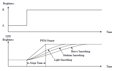
Figure 12. Smooth Function Behavior
4.
Boost Converter
4.1 Introduction
The RT4539 is a 6-CH LED driver with a boost converter. The boost converter is used to step up the input voltage to higher level. This typology consists of the components with the power switch, inductor, diode to store and release the energy at the output for the higher voltage. The application note provides the information about a boost converter built at the RT4539 IC with a 250mΩ, 36V integrated power switch and operating in the different modes by the PWM control. According to the following introduction, it gives the equations to calculate the important parameters at the power stage of a boost converter and suggests how to choose related components. Table 6 shows the boost converter specifications of the RT4539 and the electrical characteristics.
Table 6. Boost Converter Specifications
|
Parameter
|
Symbol
|
Test Conditions
|
Min
|
Typ
|
Max
|
Unit
|
|
Boost Converter
|
|
Input Supply Voltage
|
VIN
|
|
2.7
|
3.8
|
24
|
V
|
|
Switching Frequency Accuracy
|
fSW_ACC
|
Boost operates at PWM mode,
fSW = 600kHz
|
-10
|
--
|
10
|
%
|
|
Switching Frequency Setting Range
|
fSW_RG
|
Boost operates at PWM mode
Default = 600kHz @ 0x07h
|
0.3
|
--
|
1.6
|
MHz
|
|
Maximum Duty Cycle
|
DMAX_300kHz to 1MHz
|
fSW = 300kHz to 1MHz
|
--
|
90
|
--
|
%
|
|
DMAX_1.22MHz to 1.6MHz
|
fSW = 1.22MHz to 1.6MHz
|
--
|
95
|
--
|
|
Boost Switch RDS(ON)
|
RDS(ON)
|
|
--
|
0.25
|
--
|
Ω
|
|
Switching Current Limitation
|
IOCP
|
|
2
|
2.5
|
3
|
A
|
|
Boost Minimum on Time
|
tMON
|
|
--
|
100
|
--
|
ns
|
|
VOUT Over-Voltage Protection
|
VOVP
|
|
--
|
36
|
--
|
V
|
4.2 Duty Cycle Calculation
The maximum output voltage for the boost converter is highly based on switching the MOSFET or diode. The duty ratio (D) defines as the on-time of the MOSFET divided by the total switching period. For the boost converter, the approximate duty ratio (D) shows in the equation 2. The efficiency is added to the calculation because the converter also must consider the power dissipation. This calculation gives a result closer to the realistic statement. The maximum duty cycle of the RT4539 is around 90% when VOUT is the maximum output voltage and VIN is the minimum input voltage.
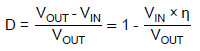
(2)
VIN = Input voltage
VOUT = Output voltage
D = Duty ratio
ƞ = Efficiency of the converter
Take 12V to 36V application as an example, the duty ratio is about 0.67. The value must not exceed the IC’s maximum duty ratio limitation. Otherwise, the output voltage of the boost converter cannot regulate normally. If the dimming mode control is selected as PWM mode or PWM-26k mode, the recommended conversion ratio is less than 0.75.
In addition to the maximum duty limitation, the RT4539 has the minimum on-time about 100ns for the boost converter. When the on-time of the boost converter is lower than the minimum on-time, the switching frequency will decrease to avoid abnormal regulation is abnormal.
4.3 Maximum Output Current
Calculating the maximum current is crucial to determine the inductor ripple current. The switch current limit in RT4539 protects the IC and circuit to avoid the damage from overcurrent. It clamps the peak inductor current. Therefore, the current ripple in a boost converter can be subtracted from the maximum current. Also, the maximum output current helps us to decide the appropriate inductor component. The following equations show the calculation with the related factors of the current.
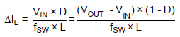
(3)
VIN = Input voltage
VOUT = Output voltage
D = Duty ratio
fSW = Switch frequency
L = Selected inductor value
After the change of the inductor current, this equation determines the maximum output current the RT4539 can deliver.

(4)
IOCP = Switching current limitation
DIL = Inductor ripple current
D = Duty ratio
The output current from the system required is necessarily less than the value of calculation. It represents the maximum current which the integrated power switch in RT4539 can withstand. The operation condition about current level recommended under the 90% of OCP level is better. If the maximum value is just little smaller the needed one, it can be solved by an inductor component with higher inductance. The higher inductance reduces the ripple current and increases the maximum output current.
4.4 Inductor Selection
The inductor plays a key role in the switching converter. It influences steady-state operation, transient response, and stability. We must consider important inductor specifications, such as inductor value, DC resistance, and saturation current when choosing the inductor component. The value of an inductor determines its ripple current. The higher inductance, the maximum current becomes higher because of reduced ripple current. The smaller inductance, the smaller size inductor can be used. It is recommended that the ripple current is set to 20% to 40% of the output DC current.
Inductor values commonly have ±20% tolerance with no current bias. When the inductor current approaches saturation level, its inductance may decrease 20% to 35%. In addition, inductors with low DCR values provide much more output current and higher conversion efficiency. The following equation is an estimation for the inductor.
(5)
VIN = Input voltage
VOUT = Output voltage
DIL = Inductor ripple current
fSW = Switch frequency
A suitable estimation for the inductor ripple current is 20% to 40% of the output current.
(6)
VIN = Input voltage
VOUT = Output voltage
IOUTMAX = Maximum output current
ƞ = Efficiency of the converter
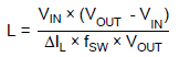
The inductance can eventually be determined by combining the equation 5 and 6 below.
(7)
VIN = Input voltage
VOUT = Output voltage
IOUTMAX = Maximum output current
ƞ = Efficiency of the converter
fSW = Switch frequency
When the boost converter operates at the boundary state, the transition is from Discontinuous Conduction Mode (DCM) to Continuous Conduction Mode (CCM). The value of the inductance can be approximated by the following equation 8.
(8)
VIN = Input voltage
VOUT = Output voltage
D = Duty ratio
fSW = Switch frequency
The inductor must be selected with a saturated current rating that is greater than the peak current as provided by the following equation 9.
(9)
VIN = Input voltage
VOUT = Output voltage
D = Duty ratio
fSW = Switch frequency
ƞ = Efficiency of the converter
L = Selected inductor value
4.5 Diode Selection
The Schottky diode is a good choice for any asynchronous boost converter with its small forward voltage. However, when selecting a Schottky diode, users must take important parameters such as power dissipation, reverse voltage rating, and pulsating peak current consideration. A suitable Schottky diode’s reverse voltage rating must be greater than the maximum output voltage, and its average rating must exceed the average output current.
4.6 Input Capacitor Selection
Low ESR ceramic capacitors recommend for input capacitor applications. Low ESR will effectively reduce the input voltage ripple caused by switching operation. Two 2.2μF low ESR ceramic capacitors are sufficient for most applications. Nevertheless, this value can decrease for applications with lower output current requirement.
Another consideration is the voltage rating of the input capacitor must be greater than the maximum input voltage.
4.7 Output Capacitor Selection
Output ripple voltage is an important index for estimating the performance. This portion consists of two parts, one is the product of IIN and ESR of output capacitor, another part is formed by charging and discharging process of output capacitor. As shown in Figure 13., DVOUT1 can evaluate based on the ideal energy equalization. According to the definition of Q, the Q value can calculate as following equation:
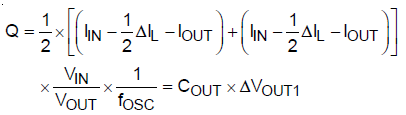
(10)
Where force is the switching frequency and DIL is the inductor ripple current. Move COUT to left side to estimate the value of DVOUT1 as the following equation:
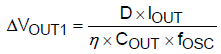
(11)
Where D is the duty cycle and ƞ is the boost converter efficiency. Finally, taking ESR into account, the overall output ripple voltage can be determined by the following equation:
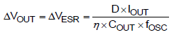
(12)
Where DVESR = DIC x RESR = IPEAK x RESR
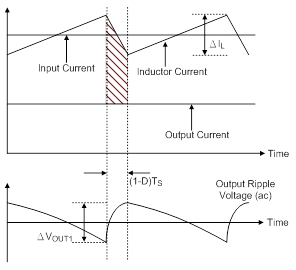
Figure 13. The Output Ripple Voltage without the Contribution of ESR
5. Layout Guideline
1. For good regulation, place the power components as close to the IC as possible. The traces should be wide and short, especially for the high current output loop.
2. The input and output bypass capacitor should be placed as close to the IC as possible and connected to the ground plane of the PCB.
3. Minimize the size of the L nodes and keep traces wide and short. Care should be taken to avoid running traces that carry any noise-sensitive signals near LX or high- current traces.
4. Separate power ground (PGND) and ground (GND). Connect the GND and the PGND islands at a single end. Make sure that there are no other connections between these separate ground planes.
5. Connect the exposed pad to a strong ground plane for maximum thermal dissipation.
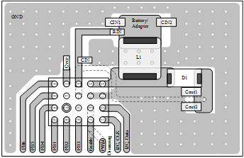
Figure 14. PCB Layout Guide